Binning is an important scientific camera feature, particularly for low-light applications such as chemiluminescence western blotting. By increasing the signal-to-noise ratio (SNR) and sensitivity, binning allows users to improve image quality, speed up acquisition times, and trade spatial resolution for enhanced sensitivity.
However, how binning is implemented varies significantly between CCD (Charge-Coupled Device) and CMOS (Complementary Metal-Oxide Semiconductor) sensors, leading to distinct performance differences.
What is binning?
In a camera sensor, individual pixels collect photons of light and convert them into electrical signals. These signals are then digitised, creating an image.
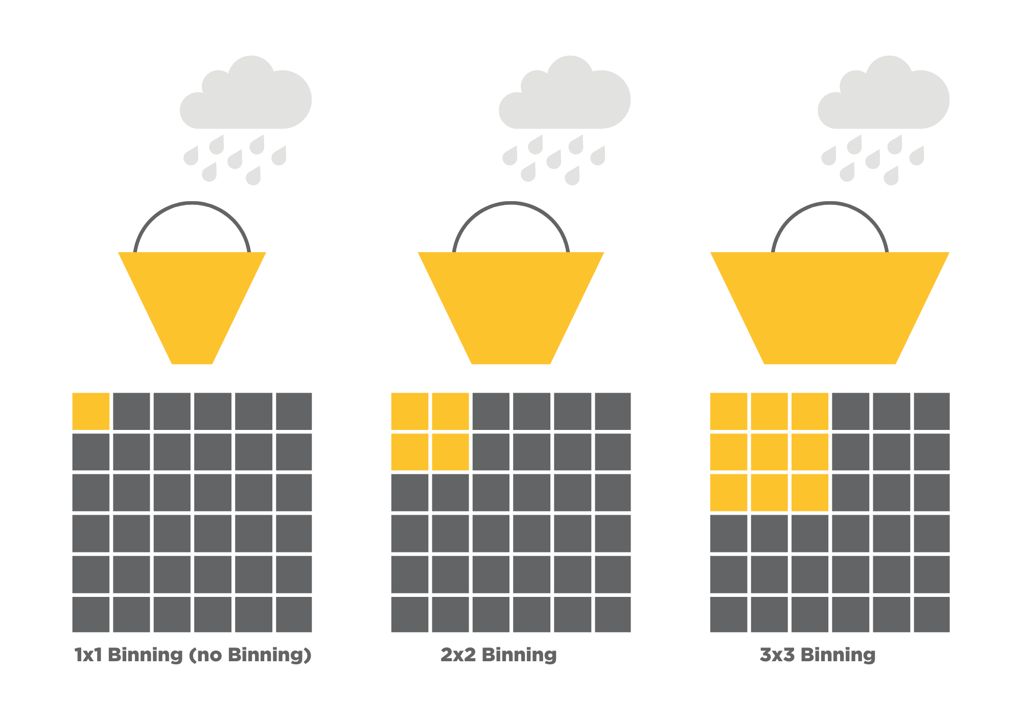
Binning combines the signals from adjacent pixels on a sensor into a single, larger, effective pixel (known as a “superpixel”). This process boosts sensitivity and reduces exposure times by combining the light captured by multiple pixels. However, the trade-off for binning is a reduction in spatial resolution.
The three-bucket graphic explains this with rain being captured in buckets. Larger buckets can capture more raindrops. Similarly, larger pixels, created through binning, collect more light, increasing the camera’s sensitivity.

How Does Binning Differ Between CCD and CMOS Sensors?
The architectural differences between CCD and CMOS sensors result in distinct approaches to binning, affecting their performance in a key way.
With CCD sensor technology, light hits the sensor and is converted into electrical charges that are then transferred across the sensor and read out sequentially. All binning is performed ‘on-chip’, whereas CMOS sensors convert light into electrical signals at each pixel, and binning is performed digitally after readout.
The advantage of how CCD sensors convert light into electrical charge and transfer it across the sensor is that this approach minimises the noise introduced by the readout amplifier, as the signal is read out once after binning. With CMOS sensors, each pixel has its photodiode and amplifier, meaning that pixel signals are independently amplified and digitised before binning. Therefore, readout noise is added at each pixel during the amplification and digitisation stages. CMOS binning, for this reason, does not achieve the same SNR improvements as CCD binning. There have been many advances in CMOS technology in recent years to reduce the per-pixel noise; however, CCD technology still has the advantage.
The following table highlights the key differences between CCD and CMOS binning.

Binning is a critical feature that enhances camera performance, particularly in scientific imaging applications. CCD sensors excel at binning due to their ability to combine pixel charges at the sensor level before readout, significantly improving the SNR. This makes CCDs the ideal choice for low-light applications, such as chemiluminescence Western blotting, where sensitivity and low noise are paramount.
Despite advances in CMOS technology, CCD sensors are currently preferred in low-light applications.
Explore the Syngene website to discover our range of imaging systems: https://www.syngene.com/
Contact our team of experts for more information: sales@syngene.com
